(China (Mainland))

Product Summary
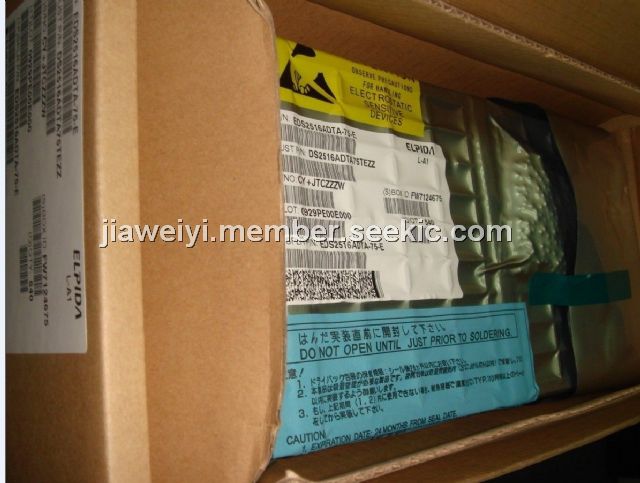
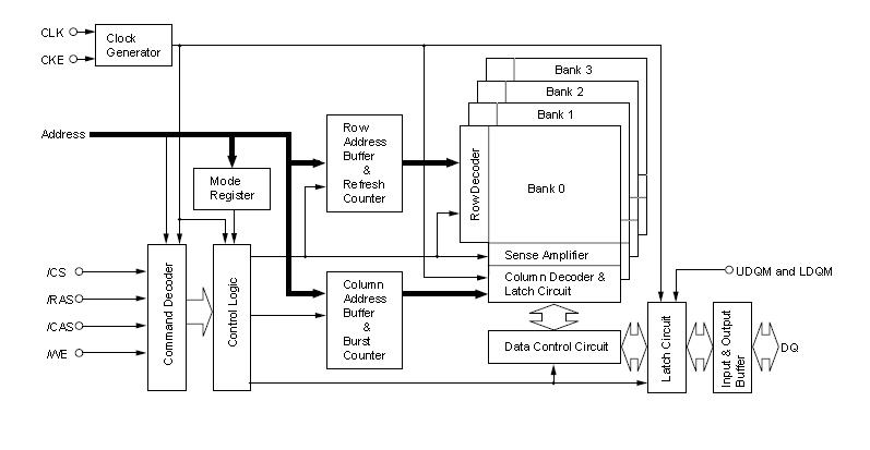
The EDS2516ADTA-75-E is 256M bits SDRAMs organized as 4,194,304 words × 16 bits × 4 banks. All inputs and
outputs are synchronized with the positive edge of the clock. It is packaged in 54-pin plastic TSOP (II). The SDRAM can perform a burst read operation. The SDRAM has a mode register that defines how it operates. The mode register is specified by the address pins (A0 to BA0 and BA1) at the mode register set cycle. For details, refer to the Mode Register Configuration.
Parametrics
Absolute maximum ratings:(1)Voltage on any pin relative to VSS:-0.5V to VDD + 0.5 (≤ 4.6 (max.));(2)Supply voltage relative to VSS:-0.5V to +4.6V;(3)Short circuit output current:50mA;(4)Power dissipation:1.0W;(5)Operating ambient temperature:0°C to 70°C;(6)Storage temperature:-55°C to +125°C.
Features
Features:(1)3.3V power supply;(2)Clock frequency: 133MHz (max.);(3)Single pulsed /RAS;(4)×16 organization;(5)4 banks can operate simultaneously and independently;(6)Burst read/write operation and burst read/single write operation capability;(7)2 variations of burst sequence;(8)Programmable /CAS latency (CL): 2, 3;(9)Byte control by UDQM and LDQM;(10)Refresh cycles: 8192 refresh cycles/64ms;(11)TSOP (II) package with lead free solder (Sn-Bi).
Diagrams
 |
 EDS2504ACTA |
Other |
|
Data Sheet |
Negotiable |
|
||||
|
EDS2504APTA |
Other |
|
Data Sheet |
Negotiable |
|
||||
|
EDS2504APTA-TI |
Other |
|
Data Sheet |
Negotiable |
|
||||
|
EDS2508ACTA |
Other |
|
Data Sheet |
Negotiable |
|
||||
|
EDS2508APSA |
Other |
|
Data Sheet |
Negotiable |
|
||||
|
EDS2508APTA |
Other |
|
Data Sheet |
Negotiable |
|
||||