(China (Mainland))

Product Summary
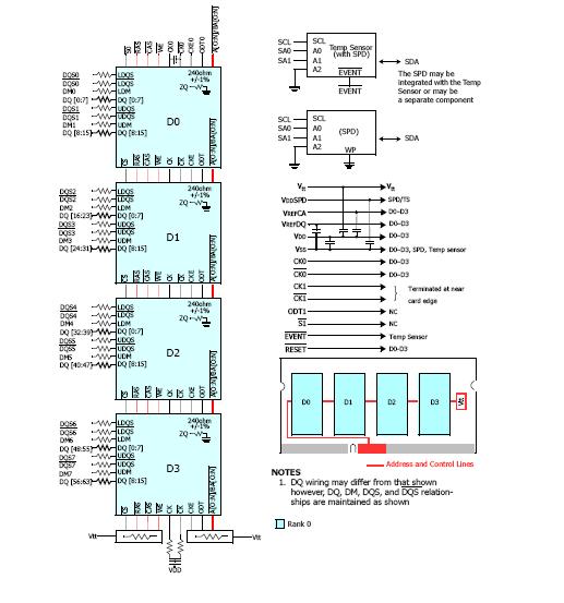
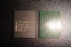
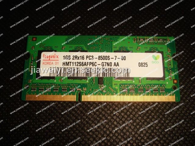
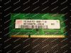
The HMT112S6AFP6C-G7N0 is a Hynix unbuffered Small Outline Dual In-Line Memory Module. It consists of 1Gb A version. DDR3 SDRAMs in Fine Ball Grid Array (FBGA) packages on a 204 pin glass-epoxy substrate. The HMT112S6AFP6C-G7N0 based on 1Gb A version provides a high performance 8 byte interface in 67.60mm width form factor of industry standard. The HMT112S6AFP6C-G7N0 is suitable for easy interchange and addition.
Parametrics
HMT112S6AFP6C-G7N0 absolute maximum ratings: (1)VDD Voltage on VDD pin relative to Vss: -0.4V to 1.975V; (2)VDDQ Voltage on VDDQ pin relative to Vss: -0.4 V to 1.975V; (3)VIN, VOUT Voltage on any pin relative to Vss: -0.4V to 1.975V; (4)TSTG Storage Temperature: -55 to +100℃.
Features
HMT112S6AFP6C-G7N0 features: (1)VDD=VDDQ=1.5V; (2)VDDSPD=3.0V to 3.6V; (3)Fully differential clock inputs (CK, /CK) operation; (4)Differential Data Strobe (DQS, /DQS); (5)On chip DLL align DQ, DQS and /DQS transition with CK transition; (6)DM masks write data-in at the both rising and falling edges of the data strobe; (7)All addresses and control inputs except data, data strobes and data masks latched on the rising edges of the clock; (8)Programmable CAS latency 5, 6, 7, 8, 9, 10, and (11) supported; (9)Programmable additive latency 0, CL-1 and CL-2 supported; (10)Programmable CAS Write latency (CWL) = 5, 6, 7, 8; (11)Programmable burst length 4/8 with both nibble sequential and interleave mode; (12)BL switch on the fly; (13)8 banks; (14)8K refresh cycles /64ms; (15)DDR3 SDRAM Package: JEDEC standard 78ball FBGA(x4/x8), 96ball FBGA(x16); (16)Driver strength selected by EMRS; (17)Dynamic On Die Termination supported; (18)Asynchronous RESET pin supported; (19)ZQ calibration supported; (20)TDQS (Termination Data Strobe) supported (x8 only); (21)Write Levelization supported; (22)Auto Self Refresh supported; (23)8 bit pre-fetch.
Diagrams