Product Summary
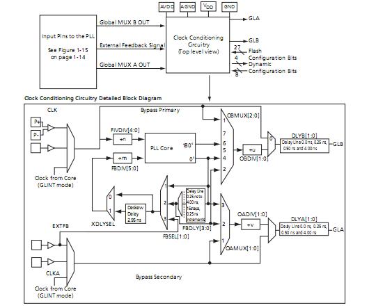
The APA300FGG256 is a Flash FPGA. It combines the advantages of ASICs with the benefits of programmable devices through nonvolatile Flash technology. The APA300FGG256 offers a unique clock conditioning circuit based on two on-board phase-locked loops (PLLs). The APA300FGG256 also offers up to one million system gates, supported with up to 198 kbits of two-port SRAM and up to 712 user I/Os, all providing 50 MHz PCI performance.
Parametrics
APA300FGG256 absolute maximum ratings: (1)Supply Voltage Core (VDD): –0.3V to 3.0V; (2)Supply Voltage I/O Ring (VDDP):–0.3V to 4.0V; (3)DC Input Voltage:–0.3V to VDDP + 0.3V; (4)PCI DC Input Voltage:–1.0V to VDDP + 1.0V; (5)PCI DC Input Clamp Current (absolute): 10 mA; (6)LVPECL Input Voltage:–0.3V to VDDP + 0.5V; (7)GND:0V.
Features
APA300FGG256 features: (1)75,000 to 1 Million System Gates; (2)27 k to 198 kbits of Two-Port SRAM; (3)66 to 712 User I/Os; (4)300, 000 to 1 million System Gates; (5)72 k to 198 kbits of Two Port SRAM; (6)158 to 712 User I/Os; (7)0.22 μm 4 LM Flash-Based CMOS Process; (8)Live At Power-Up (LAPU) Level 0 Support; (9)Single-Chip Solution; (10)No Configuration Device Required; (11)Retains Programmed Design during Power-Down/Up Cycles; (12)Mil/Aero Devices Operate over Full Military Temperature Range; (13)Low Power; (14)High Performance Routing Hierarchy.
Diagrams

 |
 APA300 |
 Other |
 |
 Data Sheet |
 Negotiable |
|
||||||
 |
 APA3002 |
 Other |
 |
 Data Sheet |
 Negotiable |
|
||||||
 |
 APA300-BG456 |
 |
 IC FPGA PROASIC+ 300K 456-PBGA |
 Data Sheet |

|
|
||||||
 |
 APA300-BG456I |
 |
 IC FPGA PROASIC+ 300K 456-PBGA |
 Data Sheet |

|
|
||||||
 |
 APA300-BGG456 |
 |
 IC FPGA PROASIC+ 300K 456-PBGA |
 Data Sheet |

|
|
||||||
 |
 APA300-BGG456I |
 |
 IC FPGA PROASIC+ 300K 456-PBGA |
 Data Sheet |

|
|
||||||
 (China (Mainland))


