Product Summary
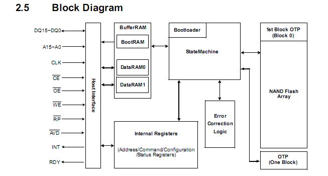
The KFG1216U2B-DIB6 OneNAND is a monolithic integrated circuit with a NAND Flash array using a NOR Flash interface. The KFG1216U2B-DIB6 includes control logic, a NAND Flash array, and 5KB of internal BufferRAM. It operates up to a maximum host-driven clock frequency of 66MHz for synchronous reads at Vcc(or Vccq. Refer to chapter 4.2) with minimum 6-clock latency. The KFG1216U2B-DIB6 is an advanced generation, high-performance NAND-based Flash memory. It integrates on-chip a single-level-cell (SLC) NAND Flash Array memory with two independent data buffers, boot RAM buffer, a page buffer for the Flash array, and a one-time-programmable block.
Parametrics
KFG1216U2B-DIB6 absolute maximum ratings: (1)Voltage on any pin relative to VSS, Vcc (for 3.3V): -0.5 to + 4.6 V; All Pins, VIN (for 3.3V): -0.5 to + 4.6 v; (2)Temperature Under Bias, Industrial Tbias: -40 to +125 ℃; (3)Storage Temperature, Tstg: -65 to +150 ℃; (4)Short Circuit Output Current, IOS: 5 mA; (5)Recommended Operating Temperature, TA (Extended Temp.): -30 to +85℃; TA (Industrial Temp.): -40 to +85℃.
Features
KFG1216U2B-DIB6 features: (1)Host Interface Type; (2)Programmable Burst Read Latency; (3)Multiple Sector Read/Write; (4)Multiple Reset Modes; (5)Multi Block Erase; (6)Low Power Dissipation; (7)Reliable CMOS Floating-Gate Technology; (8)Voltage detector generating internal reset signal from Vcc; (9)Hardware reset input (RP); (10)Data Protection Modes; (11)User-controlled One Time Programmable(OTP) area; (12)Internal 2bit EDC / 1bit ECC; (13)Internal Bootloader supports Booting Solution in system; (14)Handshaking Feature; (15)Detailed chip information.
Diagrams

 |
 KFG1216U2M |
 Other |
 |
 Data Sheet |
 Negotiable |
|
||||
 |
 KFG1216x2A-xxB5 |
 Other |
 |
 Data Sheet |
 Negotiable |
|
||||
 |
 KFG1G16D2M-DEB5 |
 Other |
 |
 Data Sheet |
 Negotiable |
|
||||
 |
 KFG1G16Q2M-DEB5 |
 Other |
 |
 Data Sheet |
 Negotiable |
|
||||
 |
 KFG1G16Q2M-DEB6 |
 Other |
 |
 Data Sheet |
 Negotiable |
|
||||
 (China (Mainland))


