Product Summary
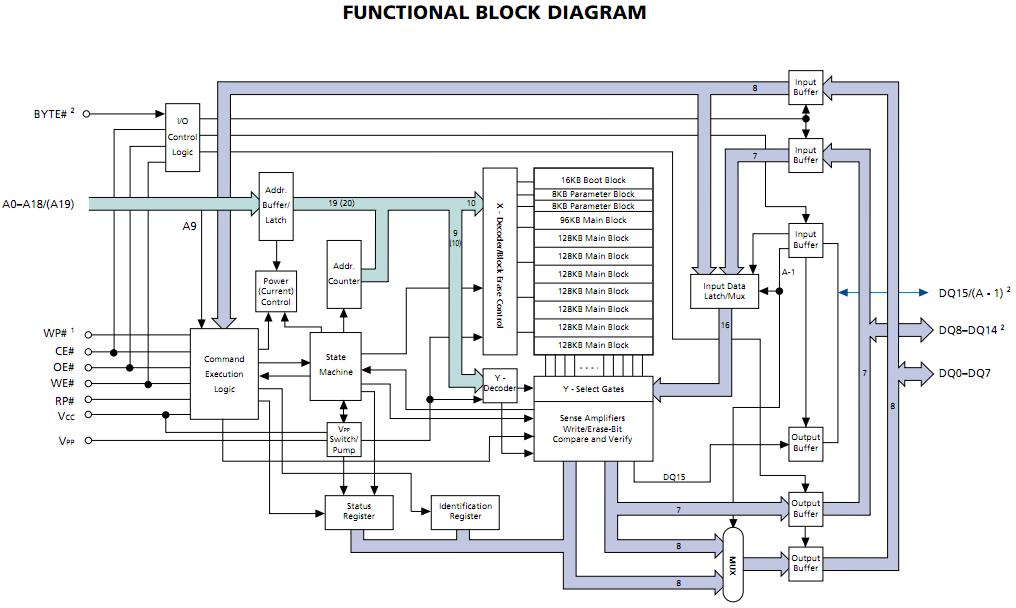
The MT28F008B3VG-9TF is a low-voltage, nonvolatile, electrically block-erasable (flash), programmable memory device containing 8,388,608 bits organized as 524,288 words (16 bits) or 1,048,576 bytes (8 bits). Writing and erasing the device is done with a VPP voltage of either 3.3V or 5V, while all operations are performed with a 3.3V VCC. Due to process technology advances, 5V VPP is optimal for application and production programming. The MT28F008B3VG-9TF is fabricated with Micron’s advanced 0.18µm CMOS floating-gate process.
Parametrics
MT28F008B3VG-9TF absolute maximum ratings: (1)Voltage on VCC Supply, Relative to VSS: -0.5V to +4V; (2)Input Voltage Relative to VSS: -0.5V to +4V; (3)VPP Voltage Relative to VSS: -0.5V to +5.5V; (4)RP# or A9 Pin Voltage, Relative to VSS: -0.5V to +12.6V; (5)Temperature Under Bias: -10 to +80℃; (6)Storage Temperature (plastic): -55 to +125℃; (7)Power Dissipation: 1W.
Features
MT28F008B3VG-9TF features: (1)Eleven erase blocks: 16KB/8K-word boot block (protected); Two 8KB/4K-word parameter blocks; Eight main memory blocks; (2)Smart 3 technology (B3): 3.3V ±0.3V VCC; 3.3V ±0.3V VPP application programming; 5V ±10% VPP application/production programming1; (3)Compatible with 0.3μm Smart 3 device; (4)Advanced 0.18μm CMOS floating-gate process; (5)Address access time: 90ns; (6)100,000 ERASE cycles; (7)Industry-standard pinouts; (8)Inputs and outputs are fully TTL-compatible; (9)Automated write and erase algorithm; (10)Two-cycle WRITE/ERASE sequence; (11)TSOP, SOP and FBGA packaging options; (12)Byte- or word-wide READ and WRITE (MT28F800B3): 1 Meg × 8/512K × 16.
Diagrams

 (China (Mainland))


