(China (Mainland))

Product Summary
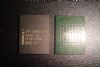
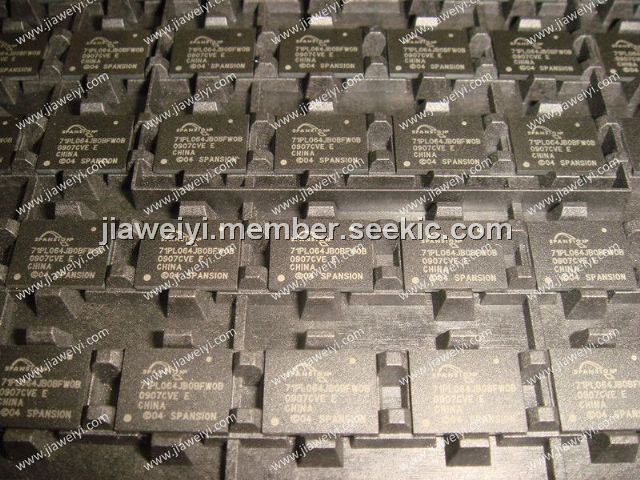
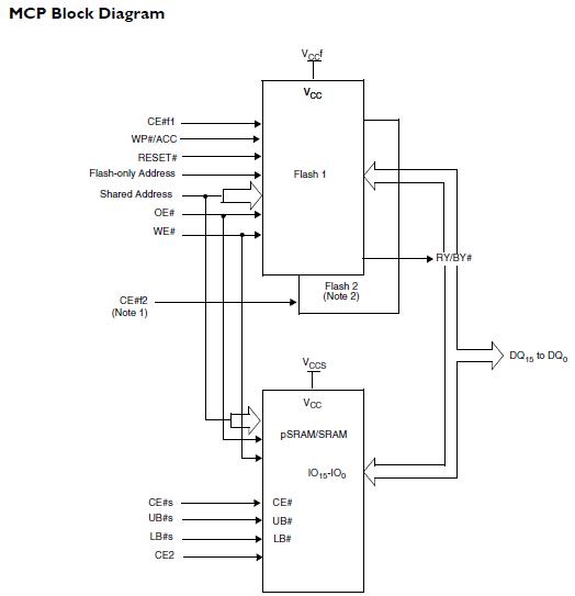
The S71PL064JB0BFW0B is a stacked Multi-Chip Product. The S71PL064JB0BFW0B consists of: One or more (Simultaneous Read/Write) Flash memory die and pSRAM or SRAM. The 256 Mb Flash memory consists of two S29PL127J devices. In this case, CE#f2 is used to access the second Flash and no extra address lines are required.
Parametrics
S71PL064JB0BFW0B flash Memory: (1)Flash Access time (ns): 65 ns; (2)(p)SRAM density: 8M SRAM; (3)(p)SRAM Access time (ns): 70 ns; (4)(p)SRAM type: SRAM1; (5)Package: TLC056.
Features
S71PL064JB0BFW0B features: (1)Power supply voltage of 2.7 V to 3.1 V; (2)High performance: 65 ns (65 ns Flash, 70 ns pSRAM); (3)Packages: 7 x 9 x 1.2mm 56 ball FBGA, 8 x 11.6 x 1.2mm 64 ball FBGA, 8 x 11.6 x 1.4mm 84 ball FBGA; (4)Operating Temperature: -25℃ to +85℃, -40℃ to +85℃.
Diagrams
 |
 S71PL256N |
Other |
|
Data Sheet |
Negotiable |
|
||||
|
S71PL254J |
Other |
|
Data Sheet |
Negotiable |
|
||||
|
S71PL2540J |
Other |
|
Data Sheet |
Negotiable |
|
||||
|
S71PL129N |
Other |
|
Data Sheet |
Negotiable |
|
||||
|
S71PL129JC0 |
Other |
|
Data Sheet |
Negotiable |
|
||||
|
S71PL129JB0 |
Other |
|
Data Sheet |
Negotiable |
|
||||