(China (Mainland))

Product Summary
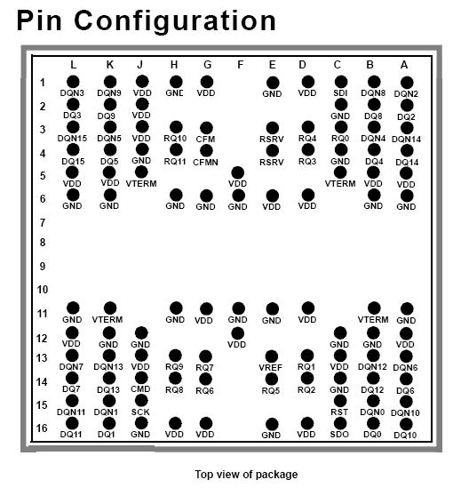
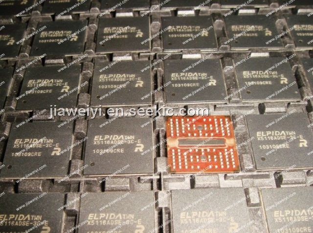
The EDX5116ADSE-3C-E is a 512M bits XDR DRAM organized as 32M words × 16 bits. It is a general-purpose high-performance memory device suitable for use in a broad range of applications. The use of Differential Rambus Signaling Level (DRSL) technology permits 4000/3200 Mb/s transfer rates while using conventional system and board design technologies. The EDX5116ADSE-3C-E is capable of sustained data transfers of 8000/6400 MB/s. The EDX5116ADSE-3C-E is packaged in 104-ball FBGA compatible with Rambus XDR DRAM pin configuration.
Parametrics
EDX5116ADSE-3C-E absolute maximum ratings: (1)θJC Junction-to-case thermal resistance: 0.5℃/Watt; (2)II,RSL RSL RQ or Serial Interface input current @ (VIN=VIH,RQ,MAX): -10 to 10μA; (3)IREF,RSL VREF,RSL current @ VREF,RSL,MAX flowing into VREF pin: -10 to 10μA; (4)VOSW,DQ DRSL DQ outputs - high-low swing: VOSW,DQ = (VOH,DQ-VOL,DQN) or (VOH,DQN-VOL,DQ): 0.200 to 0.400V; (5)RTERM,DQ DRSL DQ outputs - termination resistance: 40.0 to 60.0Ω; (6)VOL,SI RSL serial interface SDO output - low voltage: 0.0 to 0.250 V.
Features
EDX5116ADSE-3C-E features: (1)Highest pin bandwidth available 4000/3200 Mb/s Octal Data Rate (ODR) Signaling; (2)Bi-directional differential RSL (DRSL); (3)On-chip termination; (4)Highest sustained bandwidth per DRAM device; (5)Dynamic width control; (6)Low latency; (7)Low power.
Diagrams