(China (Mainland))

Product Summary
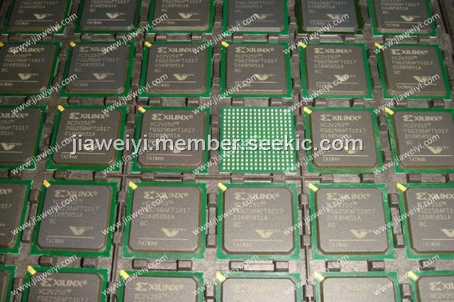
The XC2V250-6FGG256C is a platform FPGA developed for high performance from low-density to high-density designs that are based on IP cores and customized modules. The family delivers complete solutions for telecommunication, wireless, networking, video, and DSP applications, including PCI, LVDS, and DDR interfaces. The leading-edge 0.15μm / 0.12μm CMOS 8-layer metal process and the Virtex-II architecture are optimized for high speed with low power consumption. Combining a wide variety of flexible features and a large range of densities up to 10 million system gates, the XC2V250-6FGG256C enhances programmable logic design capabilities and is a powerful alternative to mask-programmed gates arrays. As shown in Table 1, the Virtex-II family comprises 12 members, ranging from 40K to 10M system gates.
Parametrics
XC2V250-6FGG256C absolute maximum ratings: (1)VCCINT Internal supply voltage relative to GND: –0.5 to 1.65V; (2)VCCAUX Auxiliary supply voltage relative to GND: –0.5 to 4.0V; (3)VCCO Output drivers supply voltage relative to GND: –0.5 to 4.0 V; (4)VBATT Key memory battery backup supply: –0.5 to 4.0 V; (5)VREF Input reference voltage: –0.5 to VCCO + 0.5 V; (6)VIN Input voltage relative to GND (user and dedicated I/Os): –0.5 to VCCO + 0.5 V; (7)VTS Voltage applied to 3-state output (user and dedicated I/Os): –0.5 to 4.0 V; (8)TSTG Storage temperature (ambient): –65 to +150 ℃; (9)TSOL Maximum soldering temperature: All regular FF/BF flip-chip and FG/BG/CS wire-bond packages: +220 ℃; Pb-free FGG456, FGG676, BGG575, and BGG728 wire-bond packages: +250 ℃; Pb-free FGG256 and CSG144 wire-bond packages: +260 ℃; TJ Maximum junction temperature: +125 ℃.
Features
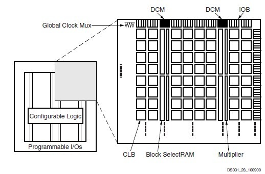
XC2V250-6FGG256C features: (1)Industry First Platform FPGA Solution; (2)IP-Immersion Architecture; (3)Densities from 40K to 8M system gates; (4)420 MHz internal clock speed (Advance Data); (5)840+ Mb/s I/O (Advance Data); (6)SelectRAM Memory Hierarchy; (7)3 Mb of True Dual-Port RAM in 18-Kbit block SelectRAM resources; (8)Up to 1.5 Mb of distributed SelectRAM resources; (9)High-performance interfaces to external memory; (10)Dedicated 18-bit x 18-bit multiplier blocks; (11)Fast look-ahead carry logic chains; (12)Up to 93,184 internal registers / latches with Clock Enable; (13)Up to 93,184 look-up tables (LUTs) or cascadable 16-bit shift registers; (14)Wide multiplexers and wide-input function support; (15)Horizontal cascade chain and Sum-of-Products support; (16)Internal 3-state bussing; (17)High-Performance Clock Management Circuitry; (18)Up to 1,108 user I/Os; (19)19 single-ended standards and six differential standards; (20)Programmable sink current (2 mA to 24 mA) per I/O; (21)Supported by Xilinx Foundation. and Alliance. Series Development Systems; (22)SRAM-Based In-System Configuration; (23)0.15μm 8-Layer Metal process with 0.12 μm high-speed transistors; (24)1.5 V (VCCINT) core power supply, dedicated 3.3 V VCCAUX auxiliary and VCCO I/O power supplies; (25)IEEE 1149.1 compatible boundary-scan logic support; (26)Flip-Chip and Wire-Bond Ball Grid Array (BGA) packages in three standard fine pitches (0.80mm, 1.00mm, and 1.27mm); (27)100% factory tested.
Diagrams
| Image | Part No | Mfg | Description |  |
Pricing (USD) |
Quantity | ||||||
|---|---|---|---|---|---|---|---|---|---|---|---|---|
 |
 XC2V250-6FGG256C |
|
IC FPGA VIRTEX-II 250K 256-FBGA |
Data Sheet |
|
|
||||||
| Image | Part No | Mfg | Description | |
Pricing (USD) |
Quantity | ||||||
|
XC2V1000 |
Other |
|
Data Sheet |
Negotiable |
|
||||||
|
XC2V1000-4BG575I |
|
IC FPGA VIRTEX-II 575PBGA |
Data Sheet |
|
|
||||||
 |
XC2V1000-4BGG575C |
|
IC VIRTEX-II FPGA 1M 575-MBGA |
Data Sheet |
|
|
||||||
|
XC2V1000-4BGG575I |
|
IC FPGA VIRTEX-II 2M 575-MBGA |
Data Sheet |
|
|
||||||
|
XC2V1000-4FF896I |
|
IC FPGA VIRTEX-II 896FCBGA |
Data Sheet |
|
|
||||||
|
XC2V1000-4FFG896C |
|
IC VIRTEX-II FPGA 1M 896-FBGA |
Data Sheet |
|
|
||||||