(China (Mainland))

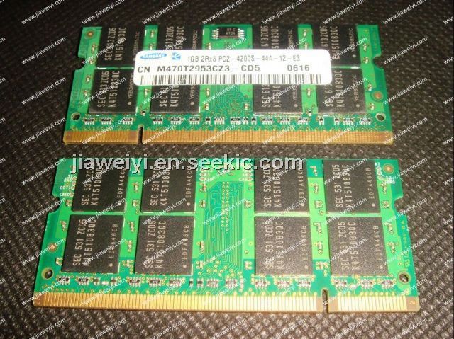
Product Summary
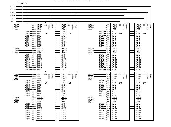
The M470T2953CZ3-CD5 is a DDR2 Unbuffered SODIMM.
Parametrics
M470T2953CZ3-CD5 absolute maximum ratings: (1)VDD Voltage on VDD pin relative to VSS: - 1.0 V to 2.3V; (2)VDDQ Voltage on VDDQ pin relative to VSS: - 0.5 V to 2.3V; (3)VDDL Voltage on VDDL pin relative to VSS: - 0.5 V to 2.3V; (4)VIN, VOUT Voltage on any pin relative to VSS: - 0.5 V to 2.3V; (5)TSTG Storage Temperature: -55 to +100℃.
Features
M470T2953CZ3-CD5 features: (1)JEDEC standard 1.8V±0.1V Power Supply; (2)VDDQ = 1.8V±0.1V; (3)200 MHz fCK for 400Mb/sec/pin, 267MHz fCK for 533Mb/sec/pin, 333MHz fCK for 667Mb/sec/pin, 400MHz fCK for 800Mb/sec/pin; (4)4 Banks; (5)Posted CAS; (6)Programmable CAS Latency: 3, 4, 5; (7)Programmable Additive Latency: 0, 1 , 2 , 3 and 4; (8)Write Latency(WL) = Read Latency(RL) -1; (9)Burst Length: 4 , 8(Interleave/nibble sequential); (10)Programmable Sequential / Interleave Burst Mode; (11)Bi-directional Differential Data-Strobe (Single-ended data strobe is an optional feature); (12)Off-Chip Driver(OCD) Impedance Adjustment; (13)On Die Termination with selectable values(50/75/150 ohms or disable); (14)PASR(Partial Array Self Refresh); (15)Average Refresh Period 7.8us at lower than a TCASE 85℃, 3.9us at 85℃<TCASE<95℃; (16)Package: 60ball FBGA - 64Mx8 , 84ball FBGA - 32Mx16; (17)All of Lead-free products are compliant for RoHS.
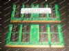
Diagrams